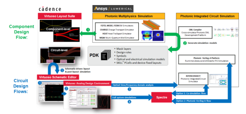
As the demand for high-speed data and advanced applications such as LIDAR and quantum computing increases, the capacity and energy efficiency challenges of photonic integrated circuits (PIC) also grow. With an ever-increasing number of components on a single photonic chip, manual techniques focused on the physical layout of components are no longer feasible. Therefore, scalable, reliable, and automated process design kit (PDK)-centric design flows are needed in photonics, as has been the case in electronics. This need for automation and standardization is demonstrated in the June 28th webinar “Design a silicon photonic ring-based WDM transceiver with EPDA.”
In electronics, IC designers can focus on their gate-level simulations, thanks to reliable and consistent software tool chains that break down the complexities of large-scale system design via multiple layers of abstraction, as well as the availability of accurate model libraries provided in foundry PDKs. Similarly, photonics has been evolving to enable scalable design from concept to a working photonic chip. In device-level simulation, physical geometry is defined, and its effects are simulated in multiple physical domains via compute intensive solvers. However, these computationally demanding simulation methods at the component level are not feasible for addressing entire photonic circuits or even single devices with large geometries. Therefore, abstract design methods are needed, where photonic devices at the component level are abstracted into compact models and represented as blocks that can be connected in a schematic design environment to create specific functionalities.
To successfully create such models, designers require seamless multiphysics simulation workflows that enable optimization of custom components with built-in capabilities to account for manufacturing variability and ensure compatibility with a foundry process. Ansys’ Lumerical suite of products enables comprehensive multiphysics simulation of photonic components, accurate time and frequency domain simulation of PICs, automated generation of statistical photonic compact model libraries (CMLs), and yield analysis, which in turn enable standardization of a PDK-centric design flow.
In addition to the challenges faced in component-level simulation, photonic circuit simulators must also capture unique optical phenomena such as amplitude and phase, wavelength, bidirectionality, and multi-modality. Moreover, photonic designs require support for curvilinear geometries, which creates complex design rule checking (DRC) and layout versus schematic (LVS) challenges. To address these challenges, Ansys Lumerical and Cadence jointly developed state-of-the-art electronic-photonic design automation (EPDA) solutions that use best-in-class photonic and electronic tools to eliminate design scaling limitations both in the front-end and back-end of the design flow.

PICs (photonic integrated circuits) incorporate various active opto-electronic components, such as lasers, photodetectors, and modulators, that require associated electronic drivers and tuning circuits. By conducting co-simulation of both the electronic and photonic circuits, one can capture the intricate interactions that occur between the optical and electrical domains. For instance, in a ring-based transceiver design, an electrical feedback loop is employed to monitor photodetectors and their associated TIA sub-circuits, which in turn are used to fine-tune the resonant wavelength of modulators. While this particular use case may not necessitate a high-speed feedback loop, there is still continuous interaction between the detection and tuning blocks. Given the multi-channel topologies of transceiver designs, designers must monitor millions of data points being exchanged between optical and electrical circuit simulators. Our webinar, “Design a Silicon Photonic Ring-Based WDM Transceiver with EPDA,” covers topics such as building compact models, curvilinear photonic layout, co-design, co-simulation, and schematic-driven layout with back-annotation.
