Flexible hybrid electronics (FHE) has the potential to combine the rigidity of traditional electronics with the flexibility of printed electronics, enabling the creation of circuits that incorporate various elements, such as printed sensors, an antenna, a thin film battery, and thin film photovoltaics. To qualify as an FHE circuit, it must possess printed and placed functionality, although not all components need to be included or printed.
The key to FHE is the integration of an integrated circuit (IC) onto a flexible substrate, which is accomplished by separately manufacturing the IC through photolithography and then linking it to printed interconnects. However, this presents some technological challenges, including the fact that silicon dies are rigid, have a different form factor, and exhibit different thermal expansion coefficients than the flexible substrate. Additionally, alternative semiconductors to silicon, such as metal oxides and organic semiconductors, have lower mobilities and are challenging to manufacture with high yields. The new IDTechEx report, “Flexible Hybrid Electronics 2020-2030: Applications, Challenges, Innovations and Forecasts,” evaluates these technical challenges, possible solutions, and other technologies necessary for the successful implementation of FHE circuits.
Temporary Solution: Packaged ICs
One possible solution to create flexible printed circuits (FPCBs) is by soldering a conventional packaged rigid IC to a stiffened flexible substrate. However, this approach hinders flexibility and is not conducive to roll-to-roll (R2R) manufacturing.
Using bare dies, which has been implemented in RFID tags, is another strategy. This involves attaching a very small IC, usually less than 1 mm2, to an antenna with conductive adhesive. Since only two electronic connections are needed, large attachment pads are viable. However, larger ICs, which are more capable and incorporate Bluetooth or memory, present challenges in terms of flexibility and conforming to the underlying substrate.
Flexible ICs from Thinned Si
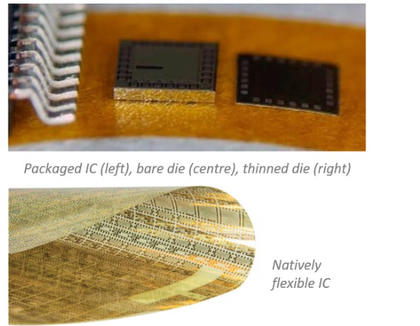
Flexible ICs are now emerging, with two different technological approaches. The first involves thinning existing Si chips by grinding them to just above the first junction. The thin die, which can be as thin as 10 um, is encapsulated in a layer of polyimide to protect it from fractures and make it easier to handle.
This methodology is applicable to many semiconducting chips, and small volumes of flexible ICs are already available for prototyping purposes. One such module measures 2.2 mm by 2.3 mm by 25 um and contains an Analog-to-Digital Converter and UHF RFID. The current limitation on flexibility is not the die itself but rather the attachment method, which is a key area for innovation. For further details, refer to the IDTechEx report “Flexible Hybrid Electronics 2020-2030: Applications, Challenges, Innovations and Forecasts”.

The above paragraph discusses the comparison between different types of integrated circuits (ICs), namely packaged, bare, and thinned silicon ICs, and natively flexible ICs. The latter is currently only available for simple applications such as RFID tags and sensor read-out. Photolithographic techniques are used to deposit metal, insulator, and metal oxide films on a polyimide substrate to create natively flexible ICs, which can cost as little as $0.01 per chip.
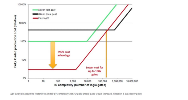
According to the provided chart, natively flexible ICs are more cost-effective to produce than Si-based ICs for applications requiring fewer than 100,000 logic gates. For instance, RFID chips can be produced for as little as $0.01 per chip, making them ideal for applications such as smart packaging, where low cost is more critical than processing power. If you are interested in learning more about these innovative technologies, you can refer to the new report from IDTechEx titled “Flexible Hybrid Electronics 2020-2030: Applications, Challenges, Innovations and Forecasts”.

To summarize, the adoption of Flexible Hybrid Electronics (FHE) necessitates alternatives to the rigid packaged ICs used in conventional rigid Printed Circuit Boards (PCBs) and Flexible PCBs (FPCBs). Thinned silicon dies, made more robust by polyimide encapsulation, are expected to be accepted in applications with more complex processing requirements, such as conventional PCB replacement. Standard bare dies may also be utilized, but they require careful handling to maintain yields. Initially, natively flexible metal-oxide based ICs, capable only of HF RFID communication and straightforward processing of sensor data, will be used in RFID tags and smart packaging applications. As the technology develops, their capabilities and range of suitable applications will likely broaden.
Our new report, titled “Flexible Hybrid Electronics 2020-2030: Applications, Challenges, Innovations and Forecasts,” provides a comprehensive overview of this emerging technology. At IDTechEx, we have been assessing and monitoring printed electronic technologies and markets for over a decade. This report is based on fresh primary research, including interviews and company visits with all the key players worldwide. It identifies and examines all the key innovation trends across material and production systems, including attachment, substrate, and metallization materials, as well as production techniques such as high-throughput pick-and-place and various S2S and R2R printing techniques.
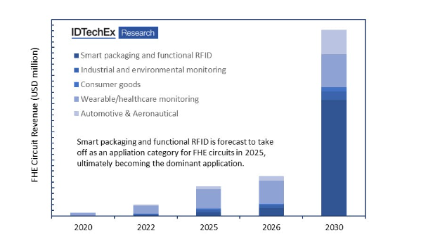
This report builds an application roadmap that illustrates how FHE will progress from simple RFID tags of today to complex flexible hybrid electronics of the future, enabling applications in smart packaging, industrial monitoring, wearable devices, and more. It provides insightful analysis into application timelines, challenges, and innovation opportunities. Furthermore, it forecasts the growth of this enabling technology, showing that the market can exceed $3 billion by 2030, with the inflection point at which rapid uptake occurs likely arriving in 2025.

